
Investigations of structure
and surface of materials
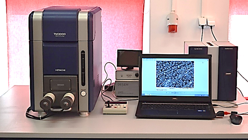
Scanning electron microscope HITACHI TM-3000 with EDS 300 Oxford attachment
The microscope is equipped with an EDS X-ray microanalyser, which enables the study of the surface morphology of samples with high resolution, as well as conducting quantitative and qualitative analysis of the chemical composition of the studied samples.
Basic technical data:
- magnification: up to 30 000x
- working conditions: 5 kV / 15 kV / EDS analysis
- state-of-the-art semiconductor BSE (backscattered electron) detector
- imaging modes: COMPO / Shadow 1 / Shadow 2 / TOPO
- maximum sample diameter: 70mm
- maximum sample height: 30mm
- simple preparation of specimens – no need for metallic plating for non-conductive samples
- possibility of stereoscopic observations with high resolution and great depth of field unattainable with optical microscopy
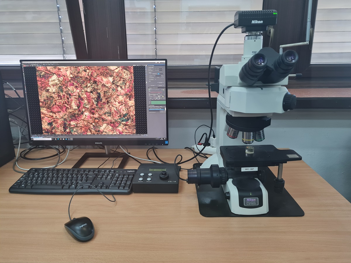
NIKON ECLIPSE LV150N metallographic microscope
Light microscope (LM) enables imaging in reflected light in bright field (BF), dark field (DF), polarized light (POL) and interference contrast so called Nomarski contrast (DIC). It has a fully motorized table (X,Y,Z), allowing automatic photography in extended depth of field (EDF), together with three-dimensional surface imaging, and also allows automatic scanning of whole metallographic scrap in high resolution.
OPERATING PARAMETERS:
- Bright (BF) and dark (DF) field observations
- Polarized light (POL) observations
- Nomarski contrast (DIC) observations
- Motorised stage
HOMMEL-TESTER T8000 Profilometer
The device allows you to perform roughness, contour and 3D topography measurements.
Main parameters:
- maximum travel length is 60 mm (with fixed resolution of 10 nm)
- adjustable speed from 0.1 to 3 mm/sec.
- probes with 2 μm tip radius
- measuring range of the instrument (in vertical direction) approx. ± 800 μm
contact and optical heads
The instrument is equipped with HommelMap Basic computer software, which enables the analysis and visualisation of the measurement data obtained.
Examples of roughness parameters possible to obtain during the test:
Ra – arithmetic mean deviation of the roughness profile. The most common Ra values for metal surfaces range from 0.02 μm to 3.5 μm – the lower the value, the more perfect the surface (0.02 μm = mirror smooth),
Rz – height of the roughness profile according to 10 points. The highest height of the roughness profile Rz is the sum of the height of the highest profile elevation and the depth of the lowest profile depression inside the elementary section.
Rp – maximum elevation of the roughness profile
Rv – depth of the lowest depression of the profile
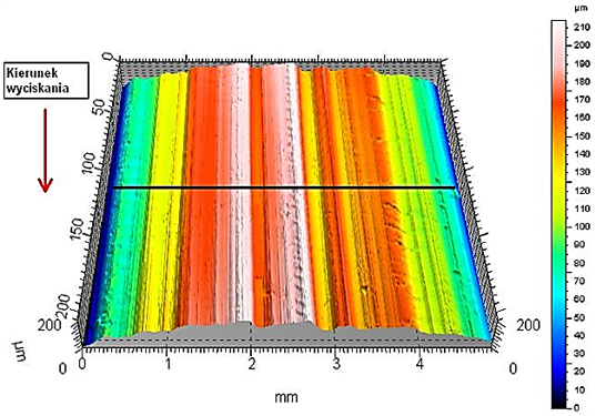
Map of surface topography
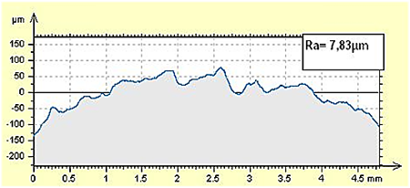
Single roughness profile